How can I verify the FPGA connections made in my Schematic, Netlist or PCB?
One of the first FPGAs I ever used on a PCB board was the XILINX XC2018… It had something like 2000 gates organized into 100 CLBS and 68 I/O Pins in a 100-pin package. To us, it was ENORMOUS! Just to set the scene properly, we were mixing these behemoths with a few Altera EP1810 devices which surprisingly enough are still available for purchase today. Those monsters had 68 pins arranged around the 4 sides of the package.
Since this was our first foray into Programmable Logic, we were quite paranoid about getting our connections right. We sat together in a room, one person with the schematic printout, and one with the printed board netlist, and one with the FPGA Pin lists. Each of us would mark the pins off with some exotic-colored highlighter (like Yellow or Yellow), and when they all checked out, we said we could ship the board.
Back in these dark ages, all the device pins were readily available on the sides of the package, and you could actually see them without a microscope. So, if we got something wrong, (AND WE DID!) we could lift a pin, add a green, blue, or red wire to fix it and be on our way to production.
At this point, I could take you through a long sorted evolutional history of FPGA usage, but let’s just fast forward 30+ years to today… We just shipped a HW design with a Xilinx UltraScale+ xcvu19p device with 1900 user assignable pins, 80 high speed transceiver blocks, and 7-10 groups of power rails, packaged into a BGA with 3824 pins. The BGA pins provide extremely limited access making it very difficult to fix mistakes with rework
To start the design, we created an initial pinout, and built our schematic Symbols with PartBuilder with the FPGA_LOGICAL flow. This gave us the ablility to easily swap the pins in the Allegro PCB Tool in order to successfully route the connections on our 24-layer board.
So how did we verify the FPGA connections before shipping the board? If we did it the old-fashioned way we’d need a huge pot of coffee, a large supply of fancy color highlighters, and more focus and patience than I’ll ever have, to cross check the 3824 connections. We’d also be tying up 2 resources for at least a day to get this job done. I don’t know about you, but my mind was not built to suffer through this kind of dreadful task.
Instead we used the NetBom's Interactive EndPoint Verification Tool (EPVT).
EPVT builds an interactive HTML report comparing the netlist connections made to the FPGA device pins, to the pin Names and voltages in the FPGA Vendors Pin Report. In this case, the Pin Report is the ‘design.pad’ file created using the ‘report_io’ command in the Xilinx Vivado Tool. The Pin Report (shown below) provides a table of information for each Pin used in the FPGA design, including the pinName, PinType, IO Standard, and the physical Pin Name of the pin. It also details the voltages that should be connected to the Power rails for the device. The Xilinx Pad file has a row for all 3824 device Pins.
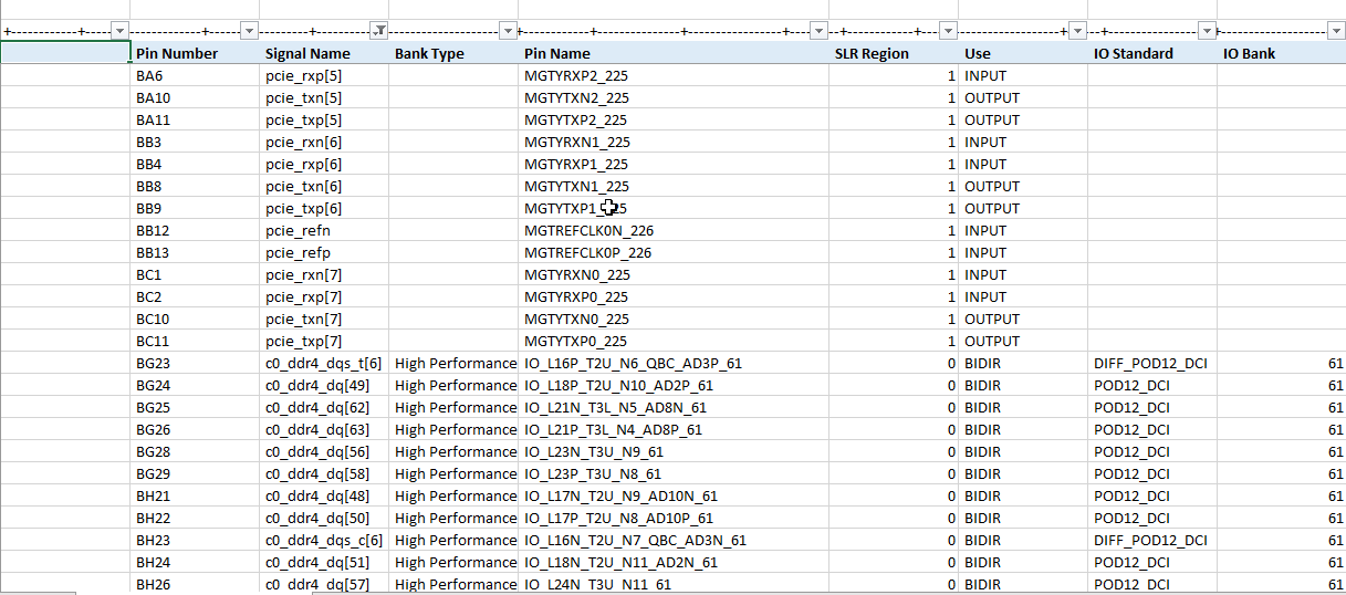
Xilinx Pad File for this Design
We configure EPVT by providing the location of the Netlist file (or Orcad Schematic, or Allegro .brd file), and the list of device EndPoints to Check.
Here we have chosen 2 devices ‘U1-XF’ and ‘U1-CPLD’.
We open another window to provide the important settings for each device.
We select XILINX FPGA for U1-XF and browse to find the device.pad file for it. We also provide a package file (which provides the generic (not design related) pinout information for the complete device). We don’t need that for Xilinx, but we do to get best results for Lattice and Intel devices, because they don’t include power and reserved pins in their Design Pin Reports.

EPVT configuration screens
When you press the Endpoint Verify button, NetBom goes to work. It reads the input netlist, finds and stores off all the connections made to U1-XF and U1-CPLD. While it is looking at connections it detects voltage nets using embedded properties or by extracting the voltage from the NetNames. Once it has the NetNames, it builds a report for both devices.
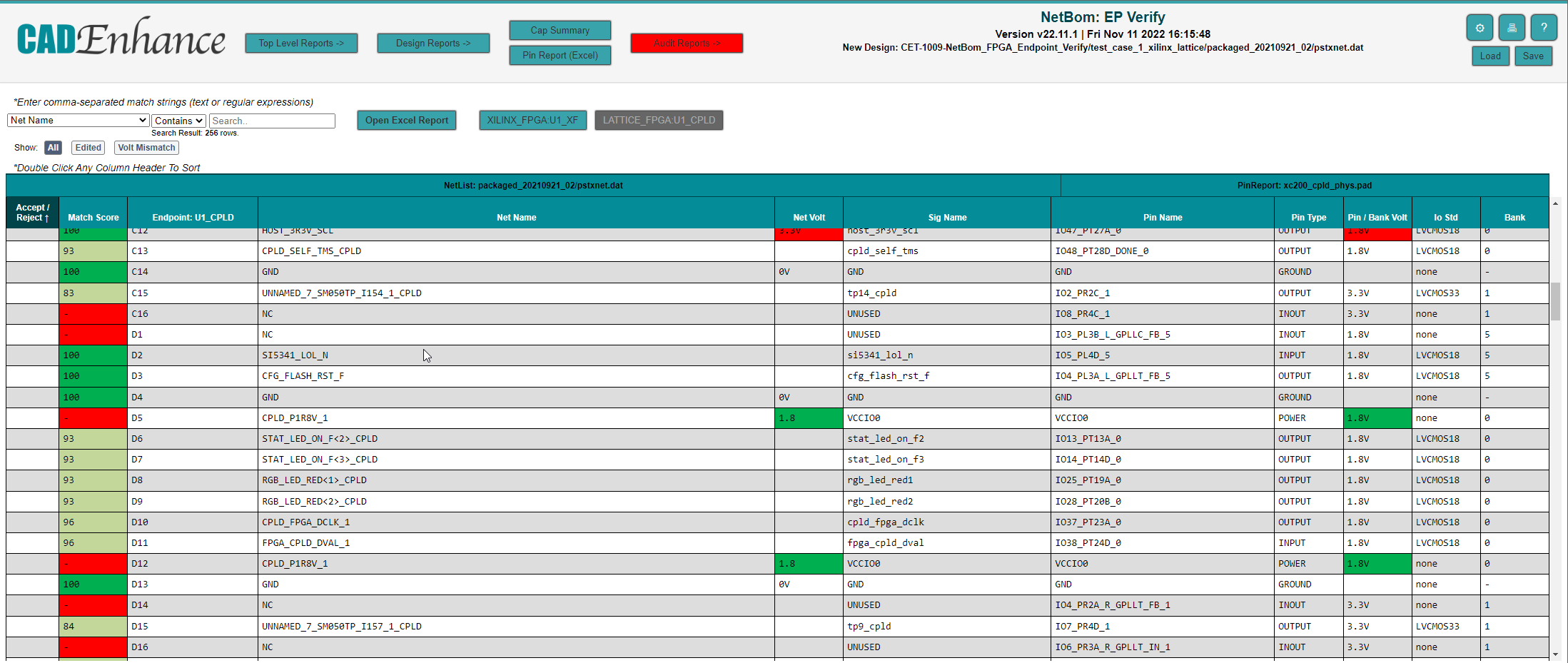
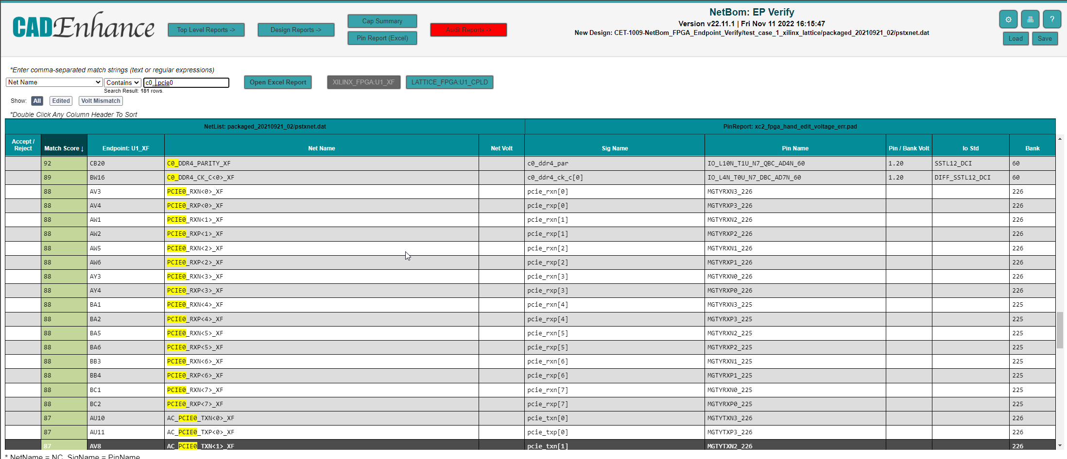
EPVT compares the netlist net name to the pin report signal name using a fuzzy matching algorithm to provide a match score for each pin. This is the first level check provided and the report can be sorted by match score to go through and work on low scores first.
EPVT also displays the voltages connected to each FPGA Bank IO pin, It compares that voltage to the voltage that was specified in the Pin Report. If the voltage is not within tolerance, those pins will be marked Red.
Once the report is generated, the user’s verification process begins. The report provides many helpful features, including filtering and sorting by any report column to help get to the root of any issues.
The filters are very flexible and support multiple match strings separated by commas so the user can focus on one or two interfaces at a time. Filters can be set find columns Containing or Not Containing the list of match strings. Matches can be a mix of simple strings and/or regular expressions for users who know how to wield that power. If the report column is numeric (for instance, the Match Score) the filters enable the user to select a range of values to search for instead.
As a substitute for those messy highlighters, we referred to earlier, the row for each device pin can be marked as Accepted/Rejected or cleared with a simple click of the mouse. The goal would be to have all rows accepted at the end of the exercise or have a good explanation for the Rejects. These annotations are stored in the browser and can be exported to save and reload when working in another browser or sharing with a colleague.
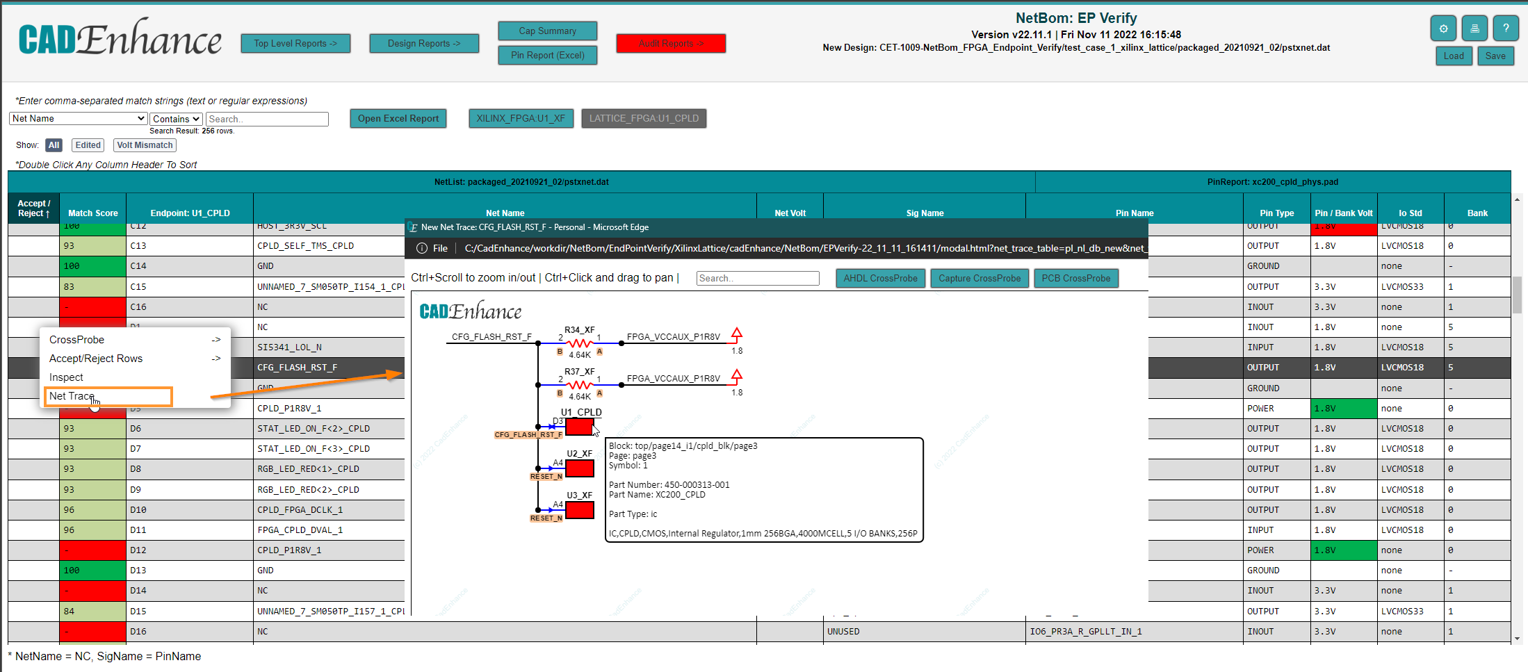
If there is any question about a pin connection, the User can right click on a row and popup a graphical trace of extended connections made to that pin in the netlist (without having to dig through the schematic to find them). Everything known about a particular device displayed in the trace can be inspected by hovering over the part.
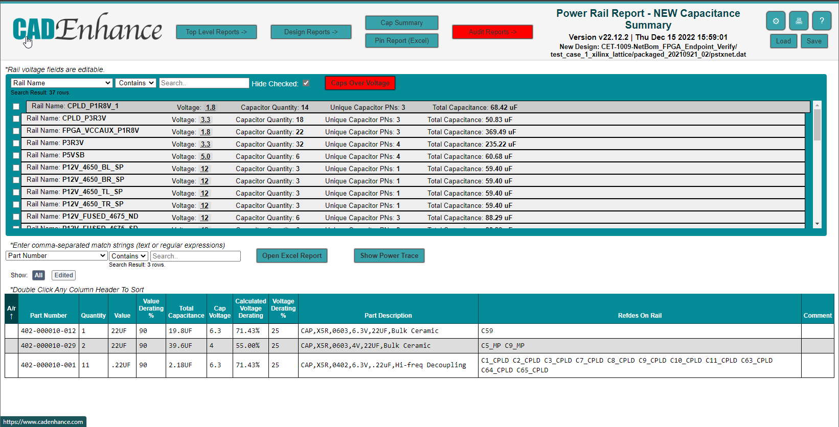
As an added bonus, for each voltage rail in the netlist, NetBom creates a detailed summary table of the bypass capacitors it detects, sorted by capacitor Value and part Number, which makes it easy to verify the device power pins are decoupled according to the Manufacturer’s requirements.
The real benefit of NetBom’s web-based reporting can be seen right here.. All we need to share the reports is a URL, so you can share them with a colleague, and we can load them on our website and share them with you. Scroll through the thumbnails below and click on one of them to interact with the real reports we generated for this blog post.